
03 / Chain stage
What are chips and HBM?
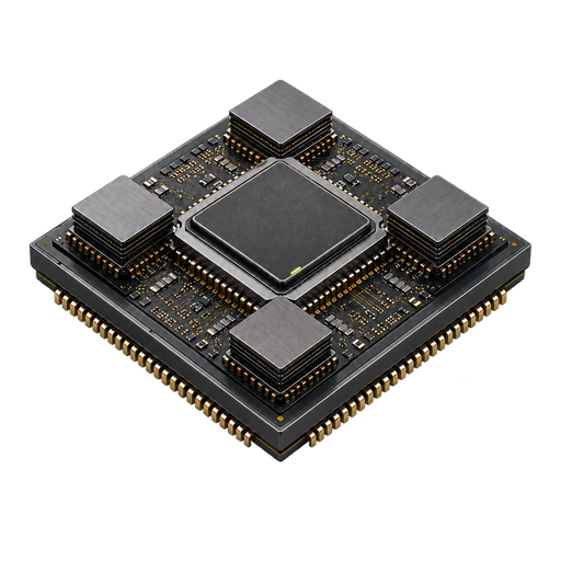
The accelerator die packaged together with high-bandwidth memory — stacks of DRAM mounted beside the processor on the same substrate — and assembled into a finished board.
(In simple terms: the compute engine, with its fast memory bolted alongside it.)
Why AI needs it
An accelerator is only as fast as the data it can be fed. Training a large model moves enormous quantities of numbers between memory and processor, so memory bandwidth, not raw arithmetic, is frequently the real limit. HBM exists to shorten that distance.
How it works
- DRAM dies are stacked vertically and wired through with vertical connections.
- The stacks are placed beside the processor die on a shared interposer.
- The assembly is packaged, tested and mounted onto an accelerator board.
- Boards are integrated into servers and then into racks.
Inputs and outputs
- Made of
- Logic dies, stacked DRAM, silicon interposers, substrates and packaging.
- Takes in
- Tested dies from the foundry and DRAM from the memory makers.
- Produces
- Packaged accelerators and finished server boards.
Where it gets stuck
Advanced packaging — the step that puts memory and logic on one substrate — is the industry's most quoted constraint. Both packaging capacity and HBM supply have repeatedly been tighter than the logic dies they serve.
A general statement about the technology. It is not a claim about any named project — where T2C can evidence a specific delay, it appears in the intelligence ledger with its source.
Where it sits in the chain



Who sells to whom. Chip designers and memory makers sell accelerators to server builders.
T2C tracks the delivery end of this chain. An upstream stage is shown as having happened — capacity cannot be billing unless the parts were made — and simultaneously as untracked, because no supplier, order or shipment record sits behind it.
Public companies in this area
T2C holds no sourced supplier record for this component yet.
Glossary
Every term that appears above, defined. Each opens in place.
-
Memory stacked beside the processor to feed it faster.
HBM
High-bandwidth memory: DRAM dies stacked vertically and placed on the same package as the processor. Shortening the distance between memory and compute is what allows an accelerator to be fed quickly enough to stay busy.
-
The shared base that links chips sitting side by side.
interposer
A silicon layer carrying dense wiring between dies mounted on it. It is what allows an accelerator and its memory stacks to be connected as though they were one chip.
-
How much data can move at once.
bandwidth
The volume of data a link can carry per second. Distinct from latency, which is how long a single message takes to arrive. A cluster can have ample bandwidth and still be slowed by latency, and the reverse.
Related signals
T2C holds no sourced signal for Chips + HBM. The intelligence ledger covers the delivery end of the chain — sites, acceptance and billing — so an upstream stage has nothing on file rather than something thin. Why coverage stops here